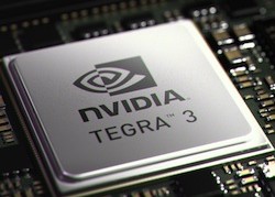
Nvidia unveiled the Tegra 3 platform last year at Mobile World Congress. Since then the chip has lived its short life mostly misunderstood. You see, it’s a quad-core chip with another 500MHz companion core that handles low-power background tasks — an architecture Nvidia previously called variable symmetric multiprocessing. But that’s a mouthful and likely a bit hard to properly market to consumers.
From here on out Nvidia wants the Tegra 3 to be called a 4-Plus-1 chip, m’kay? Nvidia even went as far as trademarking the new name.
The fifth so-called companion core is part of the Tegra 3’s popularity. It handles less strenuous tasks while the device it powers is in standby mode. Think of it as a bench player, a sixth man if you will. It’s always ready to jump, handle a bit of defense or sink a three while a starter rests.
The Tegra 3’s first birthday is coming up next week at MWC where it will no doubt be commemorated by the announcement of several high-profile smartphone and tablet announcements. There’s nothing like working on your birthday.