Superlatives abound at Cerebras, the until-today stealthy next-generation silicon chip company looking to make training a deep learning model as quick as buying toothpaste from Amazon. Launching after almost three years of quiet development, Cerebras introduced its new chip today — and it is a doozy. The “Wafer Scale Engine” is 1.2 trillion transistors (the most ever), 46,225 square millimeters (the largest ever), and includes 18 gigabytes of on-chip memory (the most of any chip on the market today) and 400,000 processing cores (guess the superlative).

Cerebras’ Wafer Scale Engine is larger than a typical Mac keyboard (via Cerebras Systems).
It’s made a big splash here at Stanford University at the Hot Chips conference, one of the silicon industry’s big confabs for product introductions and roadmaps, with various levels of oohs and aahs among attendees. You can read more about the chip from Tiernan Ray at Fortune and read the white paper from Cerebras itself.
Superlatives aside though, the technical challenges that Cerebras had to overcome to reach this milestone I think is the more interesting story here. I sat down with founder and CEO Andrew Feldman this afternoon to discuss what his 173 engineers have been building quietly just down the street here these past few years, with $112 million in venture capital funding from Benchmark and others.
Going big means nothing but challenges
First, a quick background on how the chips that power your phones and computers get made. Fabs like TSMC take standard-sized silicon wafers and divide them into individual chips by using light to etch the transistors into the chip. Wafers are circles and chips are squares, and so there is some basic geometry involved in subdividing that circle into a clear array of individual chips.
One big challenge in this lithography process is that errors can creep into the manufacturing process, requiring extensive testing to verify quality and forcing fabs to throw away poorly performing chips. The smaller and more compact the chip, the less likely any individual chip will be inoperative, and the higher the yield for the fab. Higher yield equals higher profits.
Cerebras throws out the idea of etching a bunch of individual chips onto a single wafer in lieu of just using the whole wafer itself as one gigantic chip. That allows all of those individual cores to connect with one another directly — vastly speeding up the critical feedback loops used in deep learning algorithms — but comes at the cost of huge manufacturing and design challenges to create and manage these chips.

Cerebras’ technical architecture and design was led by co-founder Sean Lie. Feldman and Lie worked together on a previous startup called SeaMicro, which sold to AMD in 2012 for $334 million (via Cerebras Systems).
The first challenge the team ran into, according to Feldman, was handling communication across the “scribe lines.” While Cerebras’ chip encompasses a full wafer, today’s lithography equipment still has to act like there are individual chips being etched into the silicon wafer. So the company had to invent new techniques to allow each of those individual chips to communicate with each other across the whole wafer. Working with TSMC, they not only invented new channels for communication, but also had to write new software to handle chips with trillion-plus transistors.
The second challenge was yield. With a chip covering an entire silicon wafer, a single imperfection in the etching of that wafer could render the entire chip inoperative. This has been the block for decades on whole-wafer technology: due to the laws of physics, it is essentially impossible to etch a trillion transistors with perfect accuracy repeatedly.
Cerebras approached the problem using redundancy by adding extra cores throughout the chip that would be used as backup in the event that an error appeared in that core’s neighborhood on the wafer. “You have to hold only 1%, 1.5% of these guys aside,” Feldman explained to me. Leaving extra cores allows the chip to essentially self-heal, routing around the lithography error and making a whole-wafer silicon chip viable.
Entering uncharted territory in chip design
Those first two challenges — communicating across the scribe lines between chips and handling yield — have flummoxed chip designers studying whole-wafer chips for decades. But they were known problems, and Feldman said that they were actually easier to solve than expected by re-approaching them using modern tools.
He likens the challenge to climbing Mount Everest. “It’s like the first set of guys failed to climb Mount Everest, they said, ‘Shit, that first part is really hard.’ And then the next set came along and said ‘That shit was nothing. That last hundred yards, that’s a problem.’ ”
And indeed, the toughest challenges, according to Feldman, for Cerebras were the next three, since no other chip designer had gotten past the scribe line communication and yield challenges to actually find what happened next.
The third challenge Cerebras confronted was handling thermal expansion. Chips get extremely hot in operation, but different materials expand at different rates. That means the connectors tethering a chip to its motherboard also need to thermally expand at precisely the same rate, lest cracks develop between the two.
As Feldman explained, “How do you get a connector that can withstand [that]? Nobody had ever done that before, [and so] we had to invent a material. So we have PhDs in material science, [and] we had to invent a material that could absorb some of that difference.”
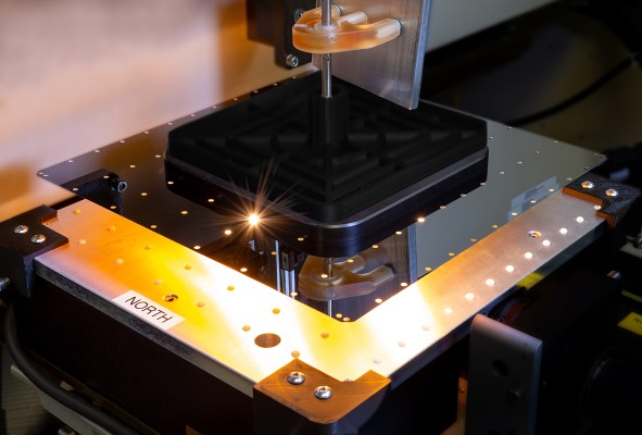
Once a chip is manufactured, it needs to be tested and packaged for shipment to original equipment manufacturers (OEMs) who add the chips into the products used by end customers (whether data centers or consumer laptops). There is a challenge though: Absolutely nothing on the market is designed to handle a whole-wafer chip.

Cerebras designed its own testing and packaging system to handle its chip (via Cerebras Systems).
“How on earth do you package it? Well, the answer is you invent a lot of shit. That is the truth. Nobody had a printed circuit board this size. Nobody had connectors. Nobody had a cold plate. Nobody had tools. Nobody had tools to align them. Nobody had tools to handle them. Nobody had any software to test,” Feldman explained. “And so we have designed this whole manufacturing flow, because nobody has ever done it.” Cerebras’ technology is much more than just the chip it sells — it also includes all of the associated machinery required to actually manufacture and package those chips.
Finally, all that processing power in one chip requires immense power and cooling. Cerebras’ chip uses 15 kilowatts of power to operate — a prodigious amount of power for an individual chip, although relatively comparable to a modern-sized AI cluster. All that power also needs to be cooled, and Cerebras had to design a new way to deliver both for such a large chip.
It essentially approached the problem by turning the chip on its side, in what Feldman called “using the Z-dimension.” The idea was that rather than trying to move power and cooling horizontally across the chip as is traditional, power and cooling are delivered vertically at all points across the chip, ensuring even and consistent access to both.
And so, those were the next three challenges — thermal expansion, packaging and power/cooling — that the company has worked around-the-clock to deliver these past few years.
From theory to reality
Cerebras has a demo chip (I saw one, and yes, it is roughly the size of my head), and it has started to deliver prototypes to customers, according to reports. The big challenge, though, as with all new chips, is scaling production to meet customer demand.
For Cerebras, the situation is a bit unusual. Because it places so much computing power on one wafer, customers don’t necessarily need to buy dozens or hundreds of chips and stitch them together to create a compute cluster. Instead, they may only need a handful of Cerebras chips for their deep-learning needs. The company’s next major phase is to reach scale and ensure a steady delivery of its chips, which it packages as a whole system “appliance” that also includes its proprietary cooling technology.
Expect to hear more details of Cerebras technology in the coming months, particularly as the fight over the future of deep learning processing workflows continues to heat up.