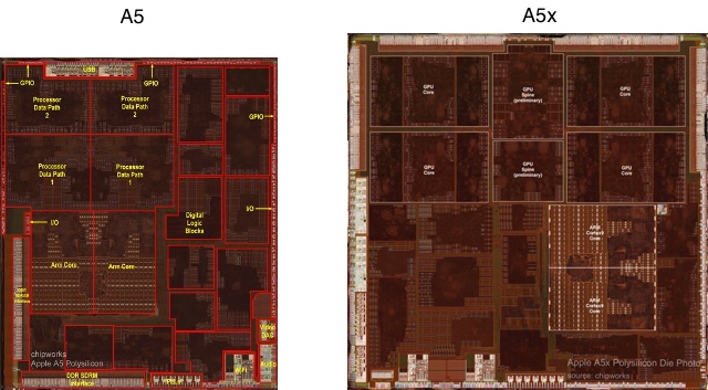
Initial teardowns of the new iPad whetted many a chip nerd’s appetite when they revealed that the A5X chip inside was truly gigantic. At nearly 13x13mm, it is significantly larger than the A5, which was itself already kind of a hefty bugger.
Now some clear images (from Chipworks) have been taken of the die itself (some rather rough ones with initial “floorplans” showed up earlier over the weekend) and it’s becoming more and more clear that the A5X is a stopgap measure: a last-generation product that’s overcompensating, if you will, with a jumbo-sized GPU.
 The A5X is manufactured with a Samsung 45nm process, a size Intel and AMD were using back in 2008. Nowadays all the cool kids are using 22nm. That means modern chips can fit around four times as many transistors and cells onto a piece of silicon than the technology used to create the A5X. It’s kind of ironic, since Apple has focused so much on getting four times the pixels into its displays.
Of course, it isn’t quite an apples-to-apples comparison; the ARM architecture and SoC model are a different animal than the x86 model. But it’s not going too far to say that the A5X is the processor equivalent of something like a souped-up street car from a few years back. Sure, it gets the job done, but you can’t keep adding turbos and wings forever. At some point that engine hits its limit. And while the GPU performance is good, the base technology of the A5X is starting to show its age, and the competition may use that to their advantage.
And even before the new iPad was released, the name A5X really tipped Apple’s entire hand. Our speculation was correct, and chances are the “true” successor to the A5 series will come in the new iPhone. Will it be based on ARM’s A15/A7 big.little model? Seems logical. Saving power is essential with the major GPU, screen, and LTE. It may be too late for Apple to adapt it, but anything could happen.
And it must be acknowledged that most consumers really, really don’t care what processor or chip is inside their iPad. But the drama going on behind the curtain is still interesting to those of us who do care, and as we have seen, sometimes these little technical stories shed light on long-term plans.
One last fun thing: if you go to the large photos over at Chipworks, you can actually see the varying densities of the logic cells on the dark areas. It shows up as a sort of mottled, almost sloppy look, but it is in fact highly precise engineering. All the wonders of our modern tech-based world have their base in these microscopic clusters of transistors, memory cells, and logic gates. It’s fascinating (to yours truly, at least) to see them forming this kind of micro-topography.