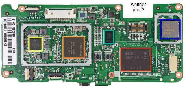
iFixit, bless their hearts, have taken a Kindle Fire to pieces, though as it turns out, there aren’t too many pieces to begin with. The battery is one huge unit, and all the processing and I/O occurs on a single PCB at the bottom of the device.
Those expecting a carbon copy of the Playbook both outside and in will be disappointed: the layout, batteries, PCB, and all the components are different, making the form factor more or less the only real similarity between the two devices.
That said, it is possible they share a processor unit; reports had TI as the supplier, and 1GHz sounds about right. Curiously, it’s not visible on the surface of the PCB, or is integrated in such a way that it can’t be identified without a more invasive teardown. But TI provided the transceivers, power manager, and so on, so it’s a safe bet. Update: yes, it was hiding under the RAM module, and it is a TI OMAP 4430, the same type used in the Playbook.

One thing they mention that I hadn’t noted before is that the battery’s charge time assumes an outlet connection for the 1.8 amps it supports; most USB ports and cables don’t provide that, so expect a longer charge time on USB (as you probably should with most devices). Total charge is stated as 4400mAh, less than the iPad 2’s 6600, but of course this has a significantly smaller screen and less intense CPU/GPU.
There don’t appear to be any hidden or unannounced features — personally, I was hoping for a microphone inside the speaker assembly, for use with Amazon’s latest acquisition. But it seems that the Fire is exactly what they say it is, no more, no less.
They’re just finishing up the teardown as I write this, and may include some extra information from Chipworks, as they have done before, so I’ll update this post if pertinent data is uncovered.
