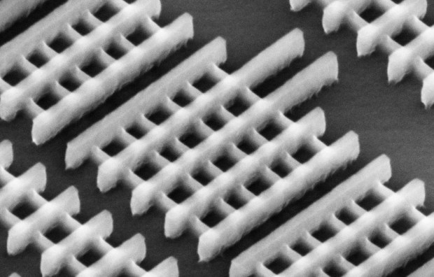
Intel has made an interesting advance in microprocessor technology after years of research, and it seems that 2011’s processors will be the first to feature 3D transistors and tri-gate technology. By optimizing the shape of the transistor at a nanometer level, Intel has made it possible to both reduce the size of individual transistors and improve their efficiency.
Now, it’s important to differentiate this 3D method from others under investigation, like IBM’s. This isn’t a multi-layer solution, merely a more complicated shape for the single layer of transistors we know and love. I say merely, but of course sculpting things at a near-atomic level is no joke. So what exactly is the advance here, and what will it enable?
If you’d rather not read, check out the video above. It does a good job of explaining, though there’s a bit of preamble you can skip.
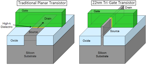
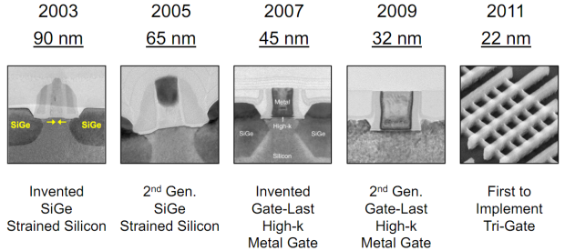
Essentially, what’s happened is this: Intel has used nano-scale architecture to move the conductive electron layer actually inside the metal component of the gate, in which the insulating layer is embedded.This illustration from their announcement deck shows it well, and the following picture is the progression of the fabrication process:


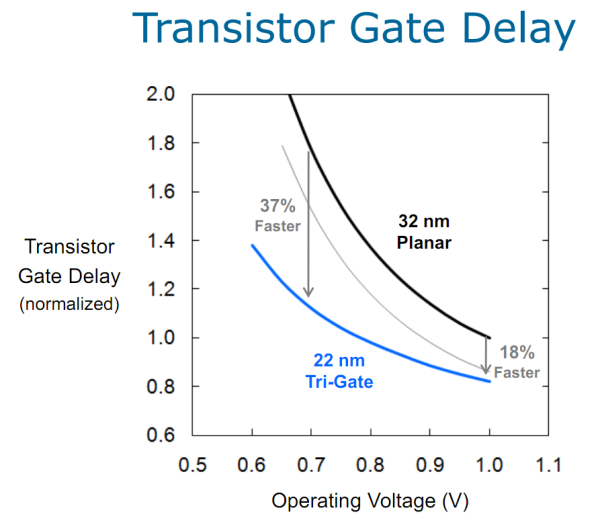
 Surrounding the electron flow on three sides, as opposed to just one, allows for improvements in just about every aspect of the transistor. Intel claims a 50% power use reduction when under load, and a 37% performance increase at low voltage, presumably from the increased rate at which these gates can open or close.
This is quite a serious leap for Intel, and immediately puts AMD further into peril, since low-power combos like Fusion have been its biggest advantage of late. It still has the lead in graphics (Intel isn’t even competitive there), but this major boost in efficiency by Intel could put them in danger on their home turf, things like all-in-ones and ultraportable laptops.
And what about ARM? This advance probably won’t hurt them. A more efficient x86 architecture is still an x86 architecture, and right now ARM is so prevalent in the portable computing market (mobile, tablet, embedded) that even a large bump to Intel’s prospects like this would take years to propagate, during which time competitors like Nvidia (Intel co-nemesis) will continue to throw in with the non-x86 option. That said, Android is perhaps the most likely to break from the pack, but that depends entirely on manufacturers, not Google, ARM, or Intel.
Intel’s roadmap for the 22nm process first mentioned Ivy Bridge, the shrink-down of current Sandy Bridge Core processors. And then there’s the low-power segment, with “Future” entrants into the various portable segments of the market. The recently-released Oak Trail generation of Atom processors will be succeeded by Clover Trail before the 22nm shift, but it’s possible they could still make it happen in mid-2012. And Intel is so marginalized in smartphone processors that I wouldn’t even hazard a guess as to their strategy there. Actually, I’d say they’ll push the mid-size segment with their low-power stuff, and then try to shrink it — the opposite of Google’s approach with Android.
The processors are due to be manufactured in the second half of 2011, though there’s no information on how or when they’ll be marketed, made available, or integrated with existing product lines.
Whatever the case, this new tech is exciting and fascinating, and I look forward to the new devices and components it enables. Nano-scale research is worth reading about no matter who’s doing it, or to what end.