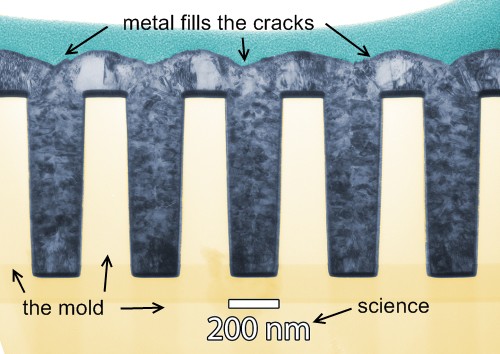
This new technique allows for making very precisely engineered little canals and then filling them with copper (or another material) leaving no gaps at all. At the scale they’re talking about, it’s essentially like laying down nano-wire in any pattern they want to create. It’s a bit like filling a mold with play-dough and then scraping off the extra.
We don’t always report hard science stuff like this, but this is interesting because I think it will have effects on some of the devices we use. After all, transistor technology is nudging the nanotech barrier (at 45nm now it’s just a few more shrinkages before classical physics give way to quantum physics) and devices like PCBs are being forced ever smaller. I don’t pretend to understand this new method, and I don’t know if it’s really even applicable, but it’s channels of conductive metal being made on an incredibly tiny scale, which makes it my business. [via Physorg]